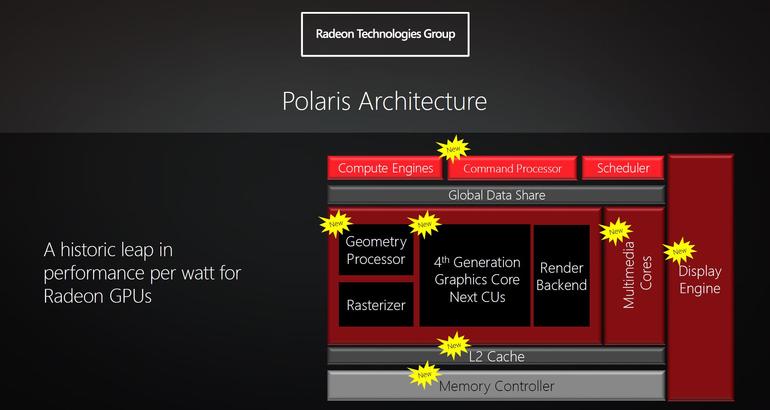
At CES this week AMD previewed its next graphics processor family–the first to employ a new process technology in five years. AMD also demonstrated a ‘mainstream’ Radeon GPU based on the new architecture meant to emphasize the new level of efficiency, or performance per watt, that the new products will deliver.

For now, AMD isn’t releasing many details on the new GPU architecture, known as Polaris, beyond the fact that it will be based on the company fourth-generation Graphics Core Next Architecture. In an interview Antal Tungler, a Senior PR Manager in AMD’s Radeon Technologies Group, said there were significant changes to the architecture in areas such as power management, cache management and the memory controllers.
Interestingly the Polaris GPU that AMD has been showing this week will use conventional graphics memory, or GDDR5, rather than the novel stacked High-Bandwidth Memory first used in AMD’s Fiji GPUs, the Radeon R9 Fury and R9 Fury X, and R9 Nano. This is most likely because HBM is still too costly to use in budget and mainstream GPUs, but there will be higher-end versions of Polaris that also use HBM. “We’re not giving up on HBM. It is actually the opposite,” Tungler said.
AMD has previously talked about some of the other features that will be supported in Polaris. These include DisplayPort 1.3, which offers 50 percent more bandwidth to support monitors with higher resolutions and refresh rates, and the latest version of HDMI, an area where it is playing catch-up with rival Nvidia. These features will also provide better support for AMD’s FreeSync variable refresh-rate technology and give the new hardware the ability to play high-dynamic range (HDR) movies. AMD also announced an improved Linux driver and plans to make many of its libraries available as open source.

But perhaps the most significant feature of Polaris is that it will be AMD’s first GPU to use smaller 3D FinFET transistors including Samsung /GlobalFoundries 14nm and TSMC 16nm. That’s because GPUs have been stuck using the same manufacturing recipe for years. The first 28nm GPU, AMD’s Radeon HD 7970, rolled out in late 2011, so by the time the first Polaris GPUs arrive in mid-2016 it will have been nearly five years on the same process. Both AMD and Nvidia skipped the disappointing 20nm planar process, which means the 14nm GPUs will have minimum features that are half the size of those on current chips.
This combined with the better control of FinFETs transistors should deliver a big boost. To illustrate this, AMD said that its early GPU delivers the same gaming performance (60 frames per second) as Nvidia’s 28nm GeForce GTX 950–available in $160 to $200 cards–while using only about 60 percent of the power. While Full HD gaming at medium-quality settings isn’t likely to excite may desktop gamers, it does mean that AMD can use the new process technology to squeeze faster 3D graphics into smaller systems such as all-in-ones and ultra-thin laptops.
AMD isn’t saying what kind of performance we can expect in a high-end GPU from the combination of the new Polaris architecture, 14nm FinFET transistors and faster HBM. Similarly Nvidia did not announce a new high-end GPU. In its CES press conference it focused exclusively on automotive technology and barely mentioned GeForce–let alone a 16nm desktop GPU (the Drive PX 2 module for cars will use two 16nm Pascal GPUs). Perhaps Nvidia is saving it for its GPU Technology Conference in April. For now the long wait for high-end GPUs using the most advanced process technology continues.


